Micron MT47H64M16NF-25E AATM Dram DDR2 1 Gbit 64M x 16bit 400 MHz Tfbga 84 Pins
MT47H64M16NF-25E AAT:M is a DDR2 SDRAM. It uses a double data rate architecture to achieve high-speed operation. The double data rate architecture is a 4n-prefetch architecture, with an interface designed to transfer two data words per clock cycle at the I/O balls. A single read or write access for the DDR2 SDRAM consists of a single 4n-bit-wide, one-clock-cycle data transfer at the internal DRAM core and four corresponding n-bitwide, one-half-clock-cycle data transfers at the I/O balls.
- Operating voltage range is 1.8V (VDD CMOS)
- 64Meg x 16 configuration, automotive qualified
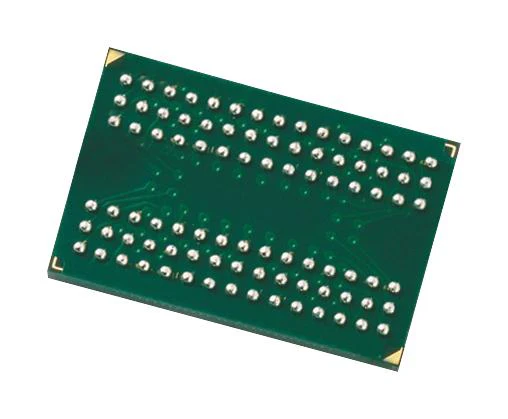
- Packaging style is 84-ball FBGA, 8mm x 12.5mm
- Timing (cycle time) is 2.5ns at CL = 5 (DDR2-800)
- Automotive temperature range is -40°C to +105°C, 8D response time
- Data rate is 800MT/s, JEDEC-standard 1.8V I/O (SSTL
- 18-compatible)
- 4n-bit prefetch architecture, duplicate output strobe (RDQS) option for x8
- Programmable CAS latency (CL), posted CAS additive latency (AL)
- WRITE latency = READ latency - 1 �CK, adjustable data-output drive strength
- 64ms, 8192-cycle refresh, supports JEDEC clock jitter specification
Other details
| Brand | MICRON |
| Part Number | MT47H64M16NF-25E AATM |
| Quantity | Each |
| Technical Data Sheet EN | |
| Product Change Notice EN |
All product and company names are trademarks™ or registered® trademarks of their respective holders. Use of them does not imply any affiliation with or endorsement by them. Image is for illustrative purposes only. Please refer to product description.
$20.99
Micron MT47H64M16NF-25E AATM Dram DDR2 1 Gbit 64M x 16bit 400 MHz Tfbga 84 Pins—
$20.99
Product Information
Product Information
Shipping & Returns
Shipping & Returns
Description
MT47H64M16NF-25E AAT:M is a DDR2 SDRAM. It uses a double data rate architecture to achieve high-speed operation. The double data rate architecture is a 4n-prefetch architecture, with an interface designed to transfer two data words per clock cycle at the I/O balls. A single read or write access for the DDR2 SDRAM consists of a single 4n-bit-wide, one-clock-cycle data transfer at the internal DRAM core and four corresponding n-bitwide, one-half-clock-cycle data transfers at the I/O balls.
- Operating voltage range is 1.8V (VDD CMOS)
- 64Meg x 16 configuration, automotive qualified
- Packaging style is 84-ball FBGA, 8mm x 12.5mm
- Timing (cycle time) is 2.5ns at CL = 5 (DDR2-800)
- Automotive temperature range is -40°C to +105°C, 8D response time
- Data rate is 800MT/s, JEDEC-standard 1.8V I/O (SSTL
- 18-compatible)
- 4n-bit prefetch architecture, duplicate output strobe (RDQS) option for x8
- Programmable CAS latency (CL), posted CAS additive latency (AL)
- WRITE latency = READ latency - 1 �CK, adjustable data-output drive strength
- 64ms, 8192-cycle refresh, supports JEDEC clock jitter specification
Other details
| Brand | MICRON |
| Part Number | MT47H64M16NF-25E AATM |
| Quantity | Each |
| Technical Data Sheet EN | |
| Product Change Notice EN |
All product and company names are trademarks™ or registered® trademarks of their respective holders. Use of them does not imply any affiliation with or endorsement by them. Image is for illustrative purposes only. Please refer to product description.